Introduction:
IC 555 TIMER is a well-known component in the electronic circles but what is not known to most of the people is the internal circuitry of the IC and the function of various pins present there in the IC. Let me tell you afact about why 555 timer is called so, the timer got its name from the three 5 kilo-ohm resistor in series employed in the internal circuit of the IC.
IC 555 timer is a one of the most widely used IC in electronics and is used in various electronic circuits for its robust and stable properties. It works as square-wave form generator with duty cycle varying from 50% to 100%, Oscillator and can also provide time delay in circuits. The 555 timer got its name from the three 5k ohm resistor connected in a voltage-divider pattern which is shown in the figure below. A simplified diagram of the internal circuit is given below for better understanding as the full internal circuit consists of over more than 16 resistors, 20 transistors, 2 diodes, a flip-flop and many other circuit components.
The 555 timer comes as 8 pin DIP (Dual In-line Package) device. There is also a 556 dual version of 555 timer which consists of two complete 555 timers in 14 DIP and a 558 quadruple timer which is consisting of four 555 timer in one IC and is available as a 16 pin DIP in the market.
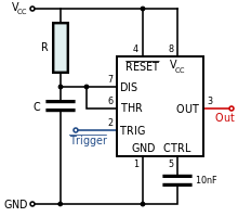
CIRCUIT DIAGRAM
Basics Concepts:
· Comparator: The Comparator are the basic electronic component which compares the two input voltages i.e. between the inverting (-) and the non-inverting (+) input and if the non-inverting input is more than the inverting input then the output of the comparator is high. Also the input resistance of an ideal comparator is infinite.
· Voltage Divider: As we know that the input resistance of the comparators is infinite hence the input voltage is divided equally between the three resistors. The value being Vin/3 across each resistor.
· Flip/Flop: Flip/Flop is a memory element of Digital-electronics. The output (Q) of the flip/flop is ‘high’ if the input at ‘S’ terminal is ‘high’ and ‘R’ is at ‘Low’ and the output (Q) is ‘low’ when the input at ‘S’ is ‘low’ and at ‘R’ is high.
Function of different Pins:-
1. Ground: This pin is used to provide a zero voltage rail to the Integrated circuit to divide the supply potential between the three resistors shown in the diagram.
2. Trigger: As we can see that the voltage at the non-inverting end of the comparator is Vin/3, so if the trigger input is used to set the output of the F/F to ‘high’ state by applying a voltage equal to or less than Vin/3 or any negative pulse, as the voltage at the non-inverting end of the comparator is Vin/3.
3. Output: It is the output pin of the IC, connected to the Q’ (Q-bar) of the F/F with an inverter in between as show in the figure.
4. Reset: This pin is used to reset the output of the F/F regardless of the initial condition of the F/F and also it is an active low Pin so it connected to ‘high’ state to avoid any noise interference, unless a reset operation is required. So most of the time it is connected to the Supply voltage as shown in the figure.
5. Control Voltage: As we can see that the pin 5 is connected to the inverting input having a voltage level of (2/3) Vin. It is used to override the inverting voltage to change the width of the output signal irrespective of the RC timing network.
6. Threshold: The pin is connected to the non-inverting input of the first comparator. The output of the comparator will be high when the threshold voltage will be more than (2/3) Vin thus resetting the output (Q) of the F/F from ‘high’ to ‘low’.
7. Discharge: This pin is used to discharge the timing capacitors (capacitors involved in the external circuit to make the IC behave as a square wave generator) to ground when the output of Pin 3 is switched to ‘low’.
8. Supply: This pin is used to provide the IC with the supply voltage for the functioning and carrying of the different operations to be fulfilled with the 555 timer.
Uses:-
The IC 55 timer is used in many circuits, for example One-shot pulse generator in Monostable mode as an Oscillator in Astable Mode or in Bistable mode to produce a flip/flop type action. It is also used in many types of other circuit for achievement of various purposes for instance Pulse Amplitude Modulatin (PAM), Pulse Width Modulation (PWM) etc
Modes
The IC 555 has three operating modes:
- BISTABLE mode or SCHMITT TRIGGER – the 555 can operate as a Flip flop, if the DIS pin is not connected and no capacitor is used. Uses include bounce-free latched switches.
- MONOSTABLE mode – in this mode, the 555 functions as a "one-shot" pulse generator. Applications include timers, missing pulse detection, bounce-free switches, touch switches, frequency divider, capacitance measurement, (PWM) and so on.
- ASTABLE (free-running) mode – the 555 can operate as an electronic oscillator. Uses include LED and lamp flashers, pulse generation, logic clocks, tone generation, security alarms, PWM and so on. The 555 can be used as a simple ADC, converting an analog value to a pulse length (e.g., selecting a THERMISTOR as timing resistor allows the use of the 555 in a temperature sensor and the period of the output pulse is determined by the temperature). The use of a microprocessor-based circuit can then convert the pulse period to temperature, linearize it and even provide calibration means.
Bistable

Schematic of a 555 in bistable mode
In bistable (also called schmitt trigger) mode, the 555 timer acts as a basic flip-flop. The trigger and reset inputs (pins 2 and 4 respectively on a 555) are held high via pull up resistor while the threshold input (pin 6) is simply floating. Thus configured, pulling the trigger momentarily to ground acts as a 'set' and transitions the output pin (pin 3) to Vcc (high state). Pulling the reset input to ground acts as a 'reset' and transitions the output pin to ground (low state). No timing capacitors are required in a bistable configuration. Pin 5 (control voltage) is connected to ground via a small-value capacitor (usually 0.01 to 0.1 μF). (discharge) is left floating.
Monostable
Schematic of a 555 in monostable mode
The output pulse ends when the voltage on the capacitor equals 2/3 of the supply voltage. The output pulse width can be lengthened or shortened to the need of the specific application by adjusting the values of R and C.
The output pulse width of time t, which is the time it takes to charge C to 2/3 of the supply voltage, is given by

where t is in seconds, R is in ohms (resistance) and C is in farads (capacitance).
While using the timer IC in monostable mode, the main disadvantage is that the time span between any two triggering pulses must be greater than the RC time constant.Conversely, ignoring closely spaced pulses is done by setting the RC time constant to be larger than the span between spurious triggers. (Example: ignoring switch contact bouncing.)
Astable

Schematic of a 555 in astable mode
In astable mode, the 555 timer puts out a continuous stream of rectangular pulses having a specified frequency. Resistor R1 is connected between VCC and the discharge pin (pin 7) and another resistor (R2) is connected between the discharge pin (pin 7), and the trigger (pin 2) and threshold (pin 6) pins that share a common node. Hence the capacitor is charged through R1 and R2, and discharged only through R2, since pin 7 has low impedance to ground during output low intervals of the cycle, therefore discharging the capacitor.
In the astable mode, the frequency of the pulse stream depends on the values of R1, R2 and C:

The high time from each pulse is given by:

and the low time from each pulse is given by:

where R1 and R2 are the values of the resistors in ohms and C is the value of the capacitor in farads.
The power capability of R
1 must be greater than

.
Particularly with bipolar 555s, low values of

must be avoided so that the output stays saturated near zero volts during discharge, as assumed by the above equation. Otherwise the output low time will be greater than calculated above. The first cycle will take appreciably longer than the calculated time, as the capacitor must charge from 0V to 2/3 of V
CC from power-up, but only from 1/3 of V
CC to 2/3 of V
CC on subsequent cycles.
To have an output high time shorter than the low time (i.e., a duty cycle less than 50%) a small diode (that is fast enough for the application) can be placed in parallel with R2, with the cathode on the capacitor side. This bypasses R2 during the high part of the cycle so that the high interval depends only on R1 and C, with an adjustment based the voltage drop across the diode. The voltage drop across the diode slows charging on the capacitor so that the high time is a longer than the expected and often-cited ln(2)*R1C = 0.693 R1C. The low time will be the same as above, 0.693 R2C. With the bypass diode, the high time is

where Vdiode is when the diode's "on" current is 1/2 of Vcc/R1 which can be determined from its datasheet or by testing. As an extreme example, when Vcc= 5 and Vdiode= 0.7, high time = 1.00 R1C which is 45% longer than the "expected" 0.693 R1C. At the other extreme, when Vcc= 15 and Vdiode= 0.3, the high time = 0.725 R1C which is closer to the expected 0.693 R1C. The equation reduces to the expected 0.693 R1C if Vdiode= 0.
The operation of RESET in this mode is not well-defined. Some manufacturers' parts will hold the output state to what it was when RESET is taken low, others will send the output either high or low.
The astable configuration, with two resistors, cannot produce a 50% duty cycle. To produce a 50% duty cycle, eliminate R1, disconnect pin 7 and connect the supply end of R2 to pin 3, the output pin. This circuit is similar to using an inverter gate as an oscillator, but with fewer components than the astable configuration, and a much higher power output than a TTL or CMOS gate. The duty cycle for either the 555 or inverter-gate timer will not be precisely 50% and will change based off any load that the output is also driving while high (longer duty cycles for greater loads) due to the fact the timing network is supplied from the devices output pin, which has different internal resistances depending on whether it is in the high or low state (high side drivers tend to be more resistive)
Specifications
These specifications apply to the NE555. Other 555 timers can have different specifications depending on the grade (military, medical, etc.).
| Supply voltage (VCC) | 4.5 to 15 V |
| Supply current (VCC = +5 V) | 3 to 6 mA |
| Supply current (VCC = +15 V) | 10 to 15 mA |
| Output current (maximum) | 200 mA |
| Maximum Power dissipation | 600 mW |
| Power consumption (minimum operating) | 30 mW@5V, 225 mW@15V |
| operating temperature | 0 to 75 °C |


.png)
